| Jumper | Function |
|
K2 | 1-2,
Pipeline mode always on. (2-3 to set pipeline mode in the CPLD
code) |
|
K101 |
Force the OTT bus access to 16 bit mode 1-2 (normally off i.e. 32 bit
mode) |
|
JP1, JP2, JP3 |
If your S-100 bus is IEEE-696 compatible these jumpers allow extra
ground access to the board. Most S-100 busses don't have this
installed |
|
JP4, JP5, JP6 |
Slave clear, POC & Reset are generated on this board (used only if
board is set as a bus master) |
|
P108 |
pHLDA to S100 bus. For slave configuration 1-2. |
|
JP103 |
Closed, Pullup resistor for pHOLD. |
|
K102 |
Normally 1-2. If 2-3 only 1MG of RAM is visible to the CPU. |
|
JP11 |
Open, pullup resistor for pHLDA |
|
K104 |
1-2 (high). If low (2-3) CPU will immediately go to a
continuous
wait state upon assuming control of the bus. This is used for
hardware debugging. |
|
JP17,19,20 & 21 |
Normally all open unless the board is a bus master. |
|
JP16 |
Normally unused. |
|
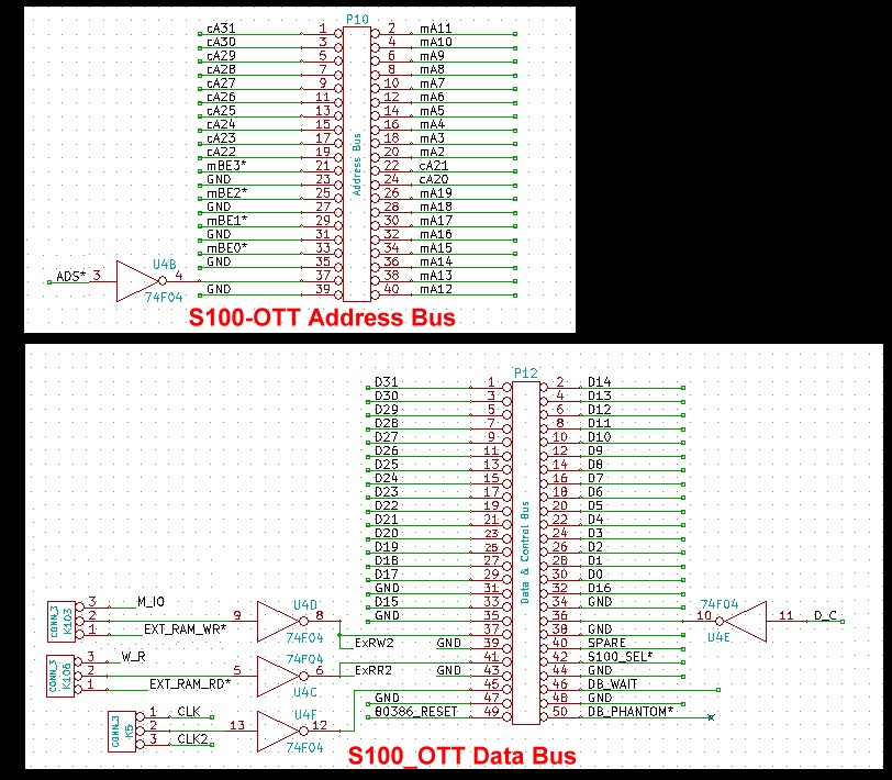
K106, K103 |
Jumpers for CPLD Rd/Wr signals to OTT RAM board. Normally 1-2 for
the V10 32/64MB RAM Board |
|
JP101 |
Disable PHI input to CPLD. Used during the initial CPLD programming
cycle where it is open. Normally closed. |
| K3 |
Normally 1-2 for board in Slave mode. 2-3 if bus master. |
|
K107 |
HOLD* signal to S100 bus. For bus slave configuration 2-3. |
|
K5 | CLK
or CLK2 signal to OTT RAM board to clock wait states. Normally 1-2
for the V10 32/64MB RAM Board |
|
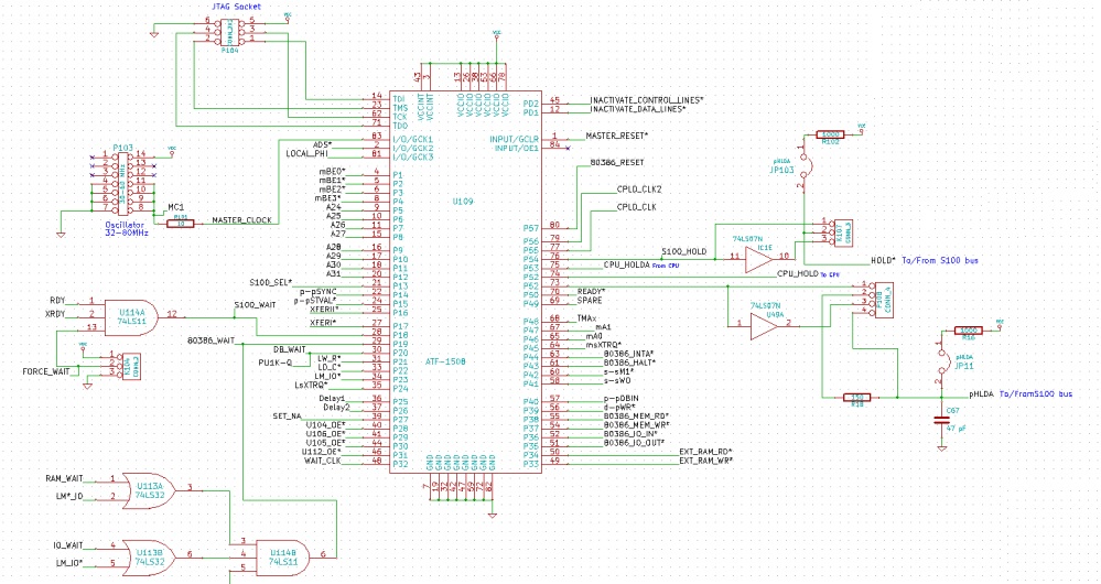
P104 |
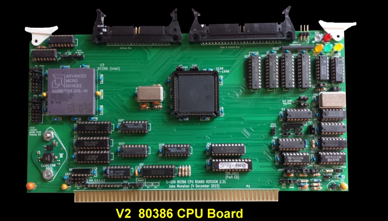
CPLD JTAJ04 programming socket for Rockfield Research 1508
programmer. Pin 1 is bottom left. |
|
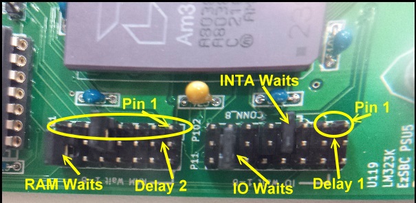
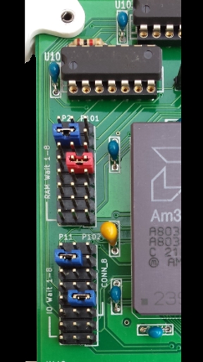
P2,P101,P11,P102 |
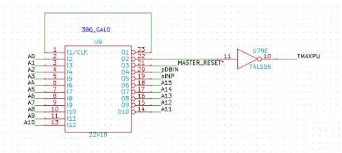
Wait state jumpers. See the above text. |
|
RR3, RR2 |
In slave
mode these pins are NOT connected to a pullup resistor network. In
master mode use 1K pullups. |